
How did you make that?
What actually happens between an idea and a working circuit board

If you’ve been reading along, you’ve already seen examples of some of the electronic projects I’ve built for real use on the farm — controllers, sensors, power systems, and things that have to survive dirt, weather, and neglect. I get asked fairly often how those projects actually come together, and what tools I use today to make them real.
There are already plenty of excellent tutorials online for getting started with electronics and PCB design, and this isn’t meant to replace any of those. Instead, I want to show my workflow: the tools I actually use, how I move from an idea to a working board, and why I make the choices I do. I’ll probably toss in a few hard-earned tips along the way, mostly so you don’t repeat all of my mistakes. That said, part of being innovative is making your own mistakes. That said, part of being innovative is making your own mistakes, and with a little luck, if you stick with this long enough, you’ll become an expert at desoldering and reworking too.
This perspective comes from roughly fifty years of building hardware, both as a hobbyist and professionally. When I first started, PCB layout meant acetate, tape, and plenty of ferric chloride, and it required a lot of patience for mess and mistakes.
Later on, we got some genuinely useful CAD tools, including DesignWorks on the Macintosh, which at the time felt like a small miracle. Even a hobbyist could draw real schematics, lay out real boards, and produce professional, manufacturing-ready output that could be sent directly to a PCB fabricator.
DesignWorks and EAGLE weren’t perfect, but they were incredibly usable. I could just get work done without wrestling the interface.
So fast forward fifty years. I’m still coding in C and Unix, still designing boards pretty much the same way. And although all the experts on the internet routinely rave about how great KiCad is, my wife makes me close my office door when I’m using it, because its inability to re-route intelligently when you move a single part is often enough to make me curse out loud.
An example project
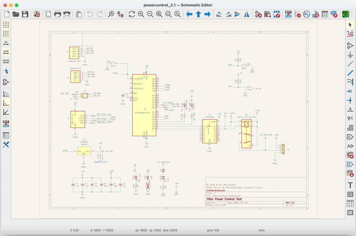
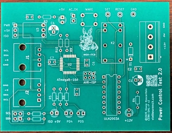
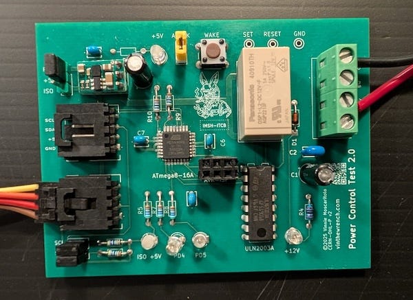
Let’s start with a small project I was working on recently. I wanted to improve the power control circuit used in my Raspberry Pi–based irrigation controller. I chose this example because it wasn’t just a hardware design exercise. It also required writing, downloading, and debugging the firmware that runs on the board.
My irrigation controller sometimes has to fall back on battery power, which means the Pi can’t be left on all the time. I needed a way to completely shut off power to the Pi, then turn it back on either periodically to perform watering tasks or automatically when AC power is restored. My previous design didn’t quite work the way I wanted, so rather than spinning a new irrigation controller board, I prototyped this as a standalone subsystem.
The subsystem communicates with the Pi over I²C and controls a small power relay. It listens for commands from the Pi and switches the relay accordingly, allowing software to shut the Pi fully off to conserve battery and bring it back up on a schedule or when AC power returns.
As with most of my projects, it started as a rough idea, became a schematic, then a board, and went through a few rounds of revision before it behaved the way I wanted.
Design approach
For this design I chose to use a simple microcontroller. Not a Linux system and not a full SBC like a Pi, just a small MCU handling the control logic. Specifically, I’m using an ATmega88PB-AU, which is part of Microchip’s AVR (Alf and Vegard’s RISC) family of microcontrollers.
It’s the same class of device people associate with Arduino-style projects, but here it has a very specific role: listen for commands over I²C and drive a latching relay that controls power to the system. I used a latching relay again, this time choosing a less expensive part than my original design. Once it’s set or reset, it holds its state without continuous power, which is exactly what you want in a battery-backed system.
At this stage I usually spend a lot of time on my favorite parts distributor sites like Mouser and Digi-Key, something I’ve been doing in one form or another since the mid-1970s. I check availability and make sure the parts I choose are likely to still exist a few years from now. This also includes downloading and digesting datasheets, and checking whether CAD symbols and footprints are already available or if I’ll need to create them myself.
A lot of design decisions get made right here, long before anything is drawn on a schematic. It’s like to look at manufacturer reference designs and sometimes search for examples where others have used the same parts, along with any feedback on how they behaved in real designs.
You do have to be selective about what you trust. Manufacturer reference designs are usually the most reliable starting point, since they reflect how the part was intended to be used and tested. Beyond that, the quality drops quickly. A lot of what you’ll find online is cargo-cult engineering. Schematics get copied without understanding, mistakes get propagated, and bad designs acquire authority simply because they’ve been repeated often enough. Anything you didn’t derive or verify yourself deserves healthy skepticism.
These days I use AI as a first-pass tool in place of search engines for this kind of research. It can be helpful for quickly finding datasheets, reference designs, and examples. BUT, you need to not only know what to ask, but also treat the results with skepticism. AI has given me some genuinely bad advice, and it will do so confidently. Anything it suggests, even pin-outs, still needs to be verified against datasheets and real designs.
In some cases, however, I’ll deliberately use pre-made modules instead of designing everything from scratch. Things like DC/DC converters are a good example. I used to spend days designing and debugging these, but these days a well-characterized module from a vendor like Pololu or Traco Power saves time, reduces risk, and lets me focus effort where it actually matters.
I plan to do a series of articles later talking about some of the parts and modules I use regularly, and why I trust them in real projects
A few rules I’ve learned the hard way
Availability beats elegance. If you can’t buy the part, the design doesn’t matter.
I prefer parts with multiple sources and long production histories.
Datasheets describe how a part is supposed to work. Errata and reference designs tell you how it actually behaves.
Assume the first board will be wrong. Make it cheap to fix and easy to debug. Add test points like you’ll need them, because you will.
Don’t get frustrated. I’ve been doing this professionally for decades and I still get things wrong. That’s part of the process.
And most of all, don’t let the bastards from internet forums like Stack Overflow, Hacker News, or Reddit get you down. Plenty of people online talk big. Most of them have never built a damn thing.

Schematic capture
Once I’ve narrowed things down a bit, it’s time to draft the schematic. These days I use KiCad. It’s an open-source tool for schematic capture and PCB layout, runs on all the major platforms, costs nothing, and is widely used, which makes sharing designs and collaborating easier. I’m not particularly happy with it, but it’s free, broadly supported, and, for better or worse, it does work. There’s also no shortage of tutorials and examples, which lowers the barrier to getting started.
As a matter of fact, I’m not really happy with any of the CAD tools these days. They’ve all become bloated, overloaded with features I rarely need, and far more complex than the problems I’m usually trying to solve.
So we’re stuck with KiCad. Cussing about it won’t make it better, and my wife will just have to close my office door again. Here are a few survival rules that have kept me sane.
Always verify your parts against the datasheet.
I’ve been burned more than once by errors in the stock component libraries. Instead, I usually pull symbols and footprints from external sources, and then verify them anyway. Sources I commonly check:
Manufacturer-provided libraries, often the most accurate when available, but not always KiCad-native
No matter where a symbol or footprint comes from, I treat it as a starting point, not a guarantee. The datasheet is still the source of truth.
Draw schematics for humans.
Make the signal flow obvious. Inputs on the left, outputs on the right. Power at the top, ground at the bottom. Group related circuitry together. Don’t be afraid to edit symbols if it improves clarity. Rearranging pins, splitting multi-unit parts, or creating a custom symbol is often better than forcing the schematic to match a generic library part. If someone can’t understand the circuit without clicking around, you won’t be able to either a week later.
Give your signals good names.
Clear net names make schematics readable and debugging tolerable. Future You will care a lot about this.
Expect KiCad to change between versions.
KiCad has a habit of moving things around and changing the way things work from release to release. It’s almost always better to finish a project than to upgrade in the middle of it.
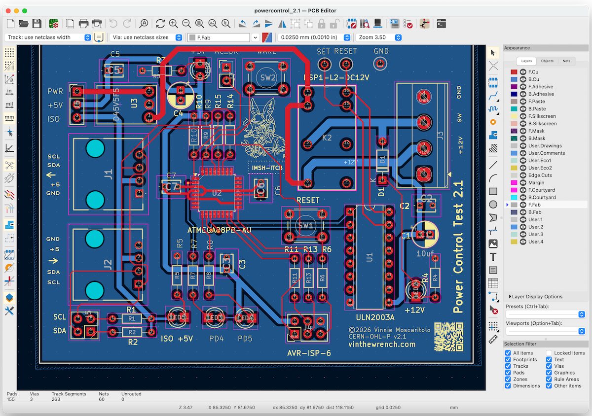
Board Layout
Schematics are the easy part. Board layout is where physics, manufacturing, and future debugging all come into play. Board layout is as much art as it is science.
At its core, board layout is a puzzle. You’re figuring out how to place parts so they make sense electrically and physically, then routing connections along the shortest, cleanest paths without painting yourself into a corner. Every move constrains the next one.
It’s a chess game. You quickly discover that the part manufacturers never talked to each other, or if they did, they conspired to make interconnection as awkward as possible.
All of this happens inside a set of engineering rules. Clearances, impedance, current density, manufacturability. Ignore them and you will fail, sometimes quickly and sometimes in subtle, intermittent ways that will cost you days.
Rules alone don’t make a good board. The art is knowing which rules matter here, which ones barely matter at all, and when violating a “best practice” is the least bad option.
I wish I could recommend a good course or book on the topic. I can’t. If there’s a single book that gets the mindset right, it’s The Art of Electronics and The Art of Electronics: The X Chapters. Not because they teach PCB layout, but because they teach judgment. The rest you learn by doing it wrong a few times. Until that happens, here are a few tips that might save you some pain.
Placement solves most problems
If you get stuck and discover you can’t get there from here without crossing layers with vias, pause and reconsider the placement. Try rotating parts, moving connectors, or swapping sides. This is especially true with surface-mount parts. Sometimes that’s all it takes.
Ground first, signals second
Every signal is a loop. Current goes out on the trace and returns through ground. If you don’t give it a clean path, it will find one anyway. On two-layer boards, keep ground solid on one side. When you have to route through it, keep cuts short, restore the pour immediately, and stitch ground with vias so return current can cross layers cleanly. If ground turns into islands, stop and rethink the placement. The goal isn’t a perfect plane. It’s a continuous return path.
You are not a robot.
Make the board something a human can build, probe, and fix. That means leaving room for fingers, probes, and tools, adding test points you can actually reach, spacing parts so rework doesn’t require luck, and placing connectors and programming headers where hands naturally go. Assume the board will be built on a bench, debugged at odd hours, and fixed at least once. Design for human mistakes, human patience, and human limits. If the board only works when assembled by a pick-and-place machine and debugged by automation, it’s a crappy design.
Bonus Tip: Silkscreen is free. Use it.
Add clear labels. Mark pin 1. Show signal names where probes will land. If there’s room, add a version number or a date so you know what you’re holding six months from now. And yes, it’s fine to have a little fun. A logo, a note, a reminder of which side is up. It doesn’t make the board less serious. It makes it more usable.
From bits to copper and fiberglass
Once the layout is done, it’s time to turn files into something real. This part is mostly about following steps. You export the fabrication files, zip them up, upload them to a board house, and wait for a box of copper and fiberglass to show up at your door.
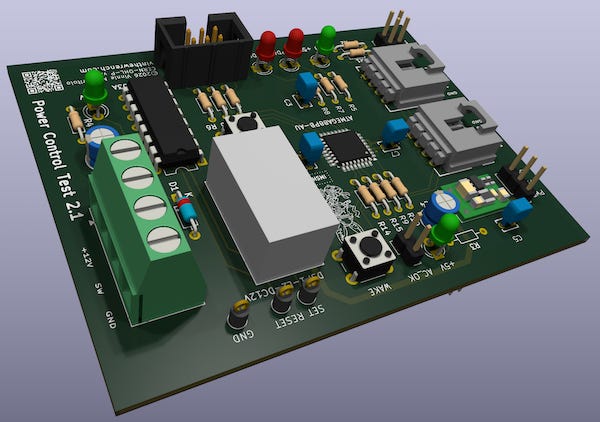
Before you upload anything, use KiCad’s 3D viewer. This one step has saved me more than once. It’s not a gimmick. It catches mistakes that are easy to miss in 2D, like reversed connectors, parts on the wrong side of the board, silkscreen colliding with pads, or footprints that technically fit but make no physical sense. Spin the board. Flip it over. Look at it like you’re about to hold it in your hands, because you will be. If something looks wrong in 3D, it is wrong.
This is the last free mistake you get before copper is involved.
Choosing a board house is mostly about what you’re optimizing for right now. Speed, cost, location, or predictability. For quick prototypes and low cost, places like JLCPCB and PCBWay are hard to beat, and there are concrete reasons why.
Both are based in China, where they sit inside a dense manufacturing ecosystem that’s been built up over decades. Board fabs, laminate suppliers, chemical processing, drilling, plating, assembly, and logistics are all clustered together. That density drives costs down and turnaround times up in ways a standalone shop in the U.S. can’t easily match. And yes, that pisses me off.
These companies behave more like software companies that happen to make PCBs. The front end is automated, quoting is instant, design rules are checked by software, and most orders flow straight through without a human in the loop. That software-first approach is what makes fast iteration cheap and predictable.
In the U.S., PCB manufacturing never reorganized around that model. Most shops evolved to serve aerospace, defense, or specialty customers, with processes optimized around custom work, sales engineers, and manual quoting. That structure makes sense for low-volume, high-margin work, but it’s the opposite of what you want when iterating quickly on prototypes.
Could this be done in the U.S.? Absolutely. Modern PCB fabrication is already highly automated. What’s missing isn’t technology, it’s willingness. Thin margins, environmental complexity, and a lack of appetite for capital-intensive manufacturing have kept anyone from building a software-first, high-throughput PCB fab here.
If you’re worried about IP, assume that anything you send to an overseas fab will be looked at. That doesn’t mean every design gets copied, but there’s no meaningful expectation of confidentiality. If that’s a problem, China is a non-starter.
I’ve also used domestic suppliers like OSH Park or PCB Unlimited For IP-sensitive work, they’re the safer choice. You pay more on the invoice, but once you factor in tariffs, customs fees, expedited international shipping, and the occasional delay, the gap often narrows. For small runs, you can sometimes break even, or at least get close.
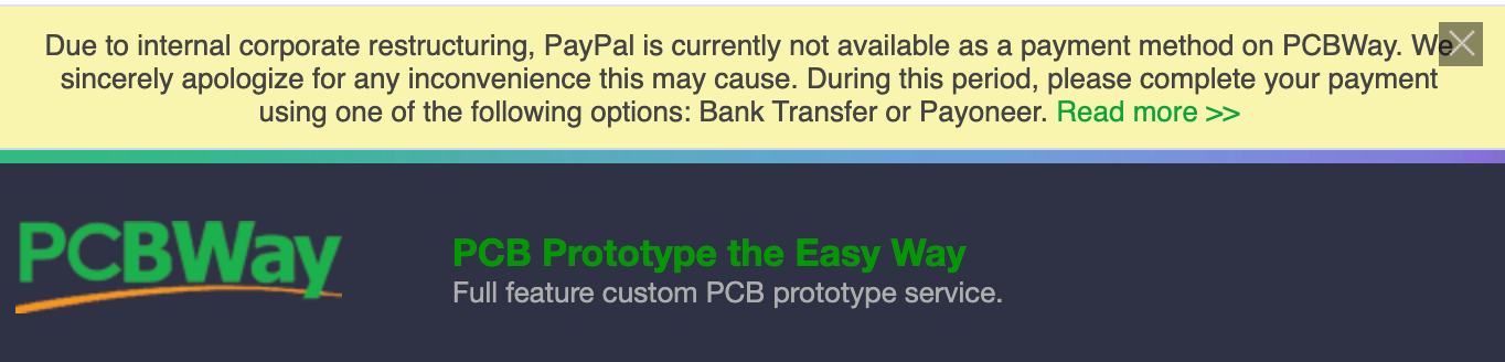
At the time of writing, PayPal pulled support for PCBWay, effectively making them unusable for many customers. This wasn’t a technical failure.
What’s really going on is that PayPal now behaves less like a payment processor and more like an unaccountable regulator. It makes unilateral risk determinations, enforces opaque compliance rules, freezes or terminates merchants without due process, and offers no meaningful appeal. These decisions aren’t about fraud or customer harm; they’re about minimizing PayPal’s own regulatory exposure. When PayPal decides a business, an industry, or a geography is inconvenient, it simply cuts them off. That kind of power, exercised without transparency or recourse, turns PayPal into a liability rather than infrastructure.
It’s also worth noting that this didn’t hit everyone equally. JLCPCB appears to have avoided the disruption largely because they don’t depend on PayPal as a primary payment rail. They diversified earlier into direct card processing and alternative settlement paths, which meant PayPal’s decision didn’t become a single point of failure. That distinction matters. When a company treats PayPal as just one option instead of critical infrastructure, PayPal loses the ability to shut the business down overnight.
When the Boards Arrive
This is the part I find the most exciting. A package arrives containing a stack of newly fabricated printed circuit boards. Now what?
The boards look great. The silkscreen is crisp. The solder mask is the right shade of green. It’s very tempting to grab the soldering iron and start populating parts immediately.
Take a breath first. Examine the boards. This is the moment to make sure the parts you plan to install will physically fit the way you expect them to, before you heat up any iron.
And trust me, I’ve screwed this up more than once. If you don’t believe me, take a look at the AVR-ISP connector on the board below. The footprint was intended to be on standard 0.1-inch centers, but it was laid out slightly off-grid. The mistake isn’t obvious in the design files, but it becomes immediately apparent when you try to fit a real connector. A standard 2×3 ISP header won’t drop into the holes without force, and shrouded or pogo adapters won’t align at all. This is the kind of error that’s trivial to catch on a bare board and deeply annoying to fix after soldering.
Preparing the Board for Soldering
Once you’re happy that the parts actually fit, it’s time to prepare the board for soldering. This part isn’t glamorous, but you’ll be grateful you did it later.
Start by cleaning the board. Even brand-new PCBs often have residue from fabrication and handling. A quick wipe with isopropyl alcohol removes oils, dust, and fingerprints that can interfere with solder wetting.
Next, inspect the pads and vias under good light. You’re looking for things like:
Solder mask encroaching on pads
Nicks or scratches in exposed copper
Mask bridges between fine-pitch pads or pins
Pads that look dull, thin, or otherwise damaged
Catching these issues now is much easier than debugging them after parts are installed.
If you’re building more than one board, this is also a good time to pick a sacrificial board for mechanical tests like enclosure fit, mounting holes, and cable clearance. It’s a bad idea to take a fully populated board anywhere near a drill press.
This is especially important when you’re using surface-mount devices, since you’ll often be working with a hot-air gun rather than an iron. It isn’t always a trivial task. On anything more complex than a simple breakout board, assembly order often involves a bit of trial and error. You don’t always know what’s going to block access to what until you’re halfway through.
In general, assemble from the flattest parts to the tallest:
Small, flat passives first
ICs and other fine-pitch components next
Connectors, switches, and tall parts last
Going through this exercise always makes me appreciate the old Heathkit manuals and their incredibly detailed, step-by-step assembly instructions. They solved this problem for you before you ever picked up a soldering iron.
Assembling the boards
For surface-mount work and inspection, a digital microscope is absolutely invaluable. It takes the guesswork out of alignment, makes fine-pitch parts manageable, and lets you catch problems like bridges or tombstoned components (where one end of a small part lifts up during reflow) before they turn into real failures.
I tried using a loupe for a while, but the real win was switching to a TOMLOV DM9. The screen is big enough and the autofocus is good enough that you can see exactly what’s happening while you place parts and while the solder flows. I don’t have to hunch over the board, and I can keep both hands free, which makes precise placement a lot easier than fighting the optics.
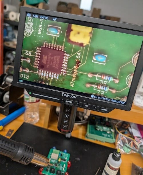
To hold the board steady under the microscope, I usually use a set of magnetic PCB pins instead of clamping it. They keep the board flat and secure, but still easy to reposition without disturbing parts that are already placed.
For actually installing the surface-mount parts, I use a hot air rework gun, in my case a TXINLEI 8858+. Unlike a soldering iron, which heats one pad at a time, a hot air gun heats the entire SMD footprint at once. That makes it much easier to seat QFNs, SOICs, and other multi-pin parts when you’re placing them by hand.
Whatever model you use, make sure it lets you control both airflow and temperature. Too much air will blow small parts out of place (ask me how I know), and too much heat will lift pads or cook nearby components.
Once I move on to through-hole parts, the tools and technique change a bit. I’ve been faithful to Weller soldering irons for decades, and after nearly thirty years I finally retired my old one and replaced it with a more modern Weller WT1010N. This is what the pros use, and yeah, it’s expensive. But I can’t emphasize enough how much good tools matter, and how much cheaper it than screwing things up because your tools suck.
I usually put the board in a PanaVise Jr., holding it vertically so I can see both the pad and the lead at the same time. Being able to rotate and tilt the board as you work keeps you from fighting gravity or burning your fingers. I’ll often tip the board slightly so the flux and solder flow into the pad instead of away from it. And remember, you don’t always have to solder from the back side. For simple parts like resistors, flowing solder from the component side can work just as well if you can see what you’re doing.
Regardless of the technique, one thing I never skimp on is flux. I wear by Kester 951 liquid soldering flux. It improves wetting, makes joints form faster, and generally turns soldering from a fight into a routine operation.
For anyone who wants to see what careful assembly really looks like, I recommend the video from CKHaun on building electronic kits. He’s a fellow I’m proud to know and someone who’s been doing this for nearly sixty years. Watching him work reminds you what doing it right looks like.
Cleaning up
Flux leaves a mess on the board, especially after surface-mount work. There is no such thing as “no-clean” flux. It all needs to be cleaned up. You’ve already spent a lot of time and money getting to this point; this is not where you cut corners or rush to be done.
First I tried scrubbing boards with brushes, soaking them in alcohol, and yes, even blasting them with brake cleaner. None of that crap really worked well. After a lot of trial and error, I finally picked up a heated ultrasonic cleaner. I’d used these before for things like carburetors and gun parts, but it turns out they work extremely well on circuit boards too.
With ultrasonic cleaning, less is more. You don’t need to cook the board or leave it in there forever. I use a mild, electronics-safe cleaning solution, strong enough to break up rosin and solder flux without being aggressive on the board or components. I keep the bath just warm, roughly 40 °C, and only run it for two to five minutes at a time. Cranking the heat or letting it run longer doesn’t clean things better, it just drives fluid under parts where you don’t want it.
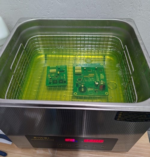
Once the board comes out of the ultrasonic bath, rinse it with clean isopropyl alcohol to flush away any residue left behind by the cleaning solution. Then I use compressed air to blow alcohol out from under connectors, ICs, and tight spots. The alcohol evaporates quickly, and the air ensures nothing gets trapped.
Done right, you end up with a board that looks as good as it works.
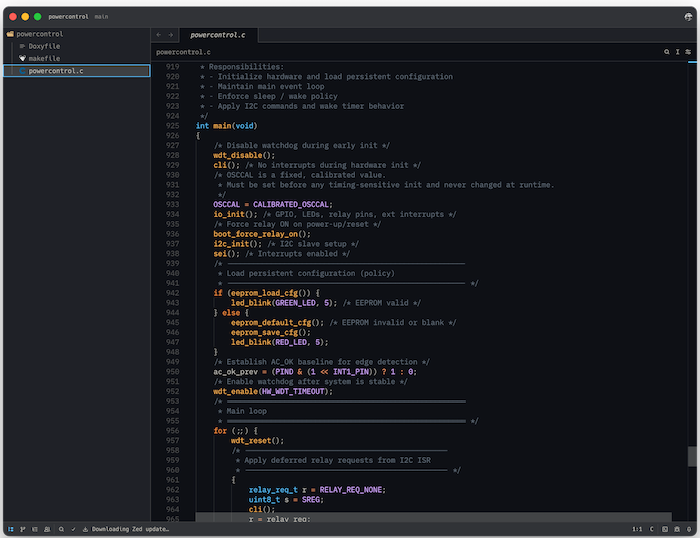
Creating the Firmware
Some of the boards I build include a microcontroller to handle the control logic. Those designs come with one extra step: writing the firmware. Without that it’s just an boat anchor until you teach it what to do.
That step has its own set of tools, just like the hardware side, and it’s worth spending a few minutes talking about what actually works for me and why.
Everyone has their own tastes and preferences, and you should use what you like. I’ve been on macOS since the first Macs came out in ’85. These days, though, I don’t use Xcode anymore. It’s bloated, heavy, and a lousy fit for what I’m building.
Instead, for AVR, Linux, or Raspberry Pi development, I’ve moved to the Zed editor. It’s fast, responsive, and focused on writing code rather than showing off the latest bouncing emojis.
Zed is a modern, high-performance code editor built by Zed Industries, a small team that knows a few things about editor design. I’ve found it to be fast and easy to customize to the way I work. The editor does one thing: it edits code, and it leaves the compiler, debugger, and toolchain where they belong, with the tools you already use.
When I’m working on Linux or Raspberry Pi systems I tend to use clang instead of GCC. On the Pis in particular, clang often compiles faster, especially during iterative builds where you’re recompiling small changes over and over. On low-power ARM cores, that faster edit–compile–test loop makes a real difference.
Clang also produces clearer diagnostics. Its warnings and error messages are generally easier to read and more precise about what actually went wrong and doesn’t send me down rabbit holes when I’m chasing bugs in C or C++ code.
For AVR work, GCC is still the right tool. The avr-gcc toolchain is the reference implementation. period. end of story.
I work directly with the toolchain instead of using the Arduino IDE because I want to see everything. Arduino is convenient, but it hides too much behind the curtain. Fuse settings, startup code, linker behavior, and compiler flags are important especially when you care about things like power consumption. I have learned over the years that if I can’t see it, I don’t trust it.
Using avr-gcc directly also means I’m in full control of the build. Everything is driven by explicit Makefiles: compiler flags, optimization levels, linker scripts, fuse checks, and flashing steps are all written down in plain text. Nothing is hidden, and nothing changes unless I change it.
Makefiles might look old-school, but they’re honest. They document exactly how a binary was produced, they’re easy to version-control, and six months later I can still see exactly what happened and why. That kind of repeatability and long-term maintainability matters, especially when you don’t want your toolchain breaking because some IDE developer decided to “improve” things on a whim. (Yes, I’m looking at you, Apple.)
Installing the AVR Toolchain
On macOS, install the toolchain with Homebrew:
brew install avr-gcc avrdudeOn Debian-based Linux systems (including Raspberry Pi OS):
sudo apt install gcc-avr binutils-avr avr-libc avrdudeThis gives you everything you actually need: the compiler, C library, binutils, and flashing tool. No IDE required.
Flashing the firmware
Once the board is assembled and the firmware is built, it’s time to get code onto the microcontroller. For AVR parts, that job is handled by avrdude.
avrdude (AVR Downloader/Uploader) is the long-standing open-source tool used to program AVR microcontrollers. It talks directly to the chip, verifies device signatures, and handles flash, EEPROM, and fuse programming.
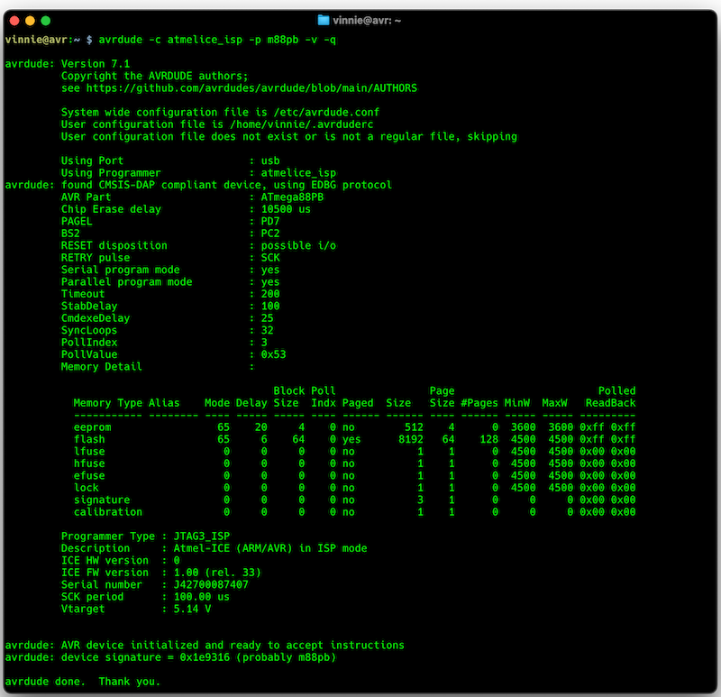
AVR parts can be programmed using either ISP (In-System Programming) or JTAG. ISP is the simpler option, using only a handful of pins and working on nearly every AVR. JTAG adds live debugging with breakpoints and single-stepping, but it costs more pins and more board complexity.
For most projects, I can get away with using ISP alone. I use an Atmel-ICE for ISP programming rather than a third-party programmer. It’s the manufacturer’s reference tool, built to match the timing, signaling, and edge cases the chips expect.
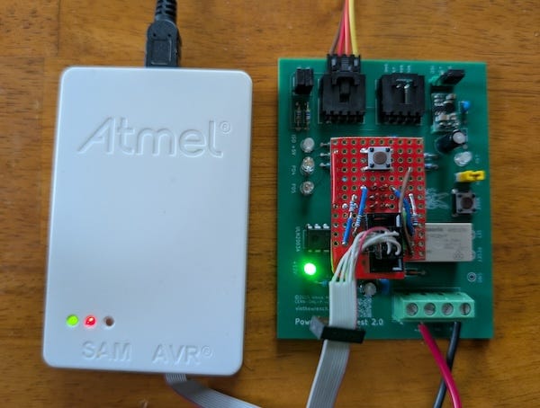
This photo shows the board being programmed using an Atmel-ICE in ISP mode. If the setup looks a little improvised, that’s because it is. Remember that earlier mistake where I got the AVR-ISP connector footprint wrong and didn’t land it on standard 0.1-inch centers? This is the consequence. I had to build a small adapter board just to mate the programmer to the header.
No, no, no, no, I don’t smoke them no more
That mistake also ended up teaching me something useful. When programming over ISP, I now make a habit of connecting the programmer to the board before applying power. Hot-plugging an ISP cable into a powered board can back-feed signals through protection diodes or I/O pins in ways the chip really doesn’t appreciate. Sometimes you get away with it. Sometimes you don’t. I didn’t, three times.
After toasting enough parts to learn the lesson properly, I started adding series resistors on the ISP lines in my later designs. This isn’t a substitute for bad habits but it does help when I screw up. This particular board predated that change, which is why the resistors were necessary.
Why I made that.
This article was titled “How Did You Make That?” because that’s the question I get most often. But right behind it is another one that matters just as much: why.
I didn’t build this as a product, a kit, or a demo. I built it because there was a real problem on our farm that needed a solution I could trust. I learned a lot along the way and stood on the shoulders of giants. It felt like the right time to give something back.
I was lucky enough to grow up at a time when people shared what they built. I still remember a guy from DEC mailing me the schematics for a PDP-8 simply because he was happy that a kid was interested. That kind of generosity mattered. I spent hours poring over schematics and code, trying to understand how things worked. That hacker ethos shaped how I learned and how I still think about building things.
That experience stuck with me. Publishing this design is my way of paying it forward, which is why I write these articles and put my work on GitHub as open source. Both the firmware and the hardware are open, under permissive licenses that let you use, modify, and build on the work and pretty much do whatever you want.
If you care about how things are made and why they’re built the way they are, you’ll probably like the rest of what I write about. Hitting like and sharing helps real people find the work. The algorithm can go pound sand.
Wow, the part about innovation and making your own mistakes realy resonated. Sounds like many of us are on our way to becoming desoldering experts!
NOTE: If avrdude works with sudo but fails as a normal user,
you likely have a USB permission issue.
The Atmel-ICE (VID 03eb, PID 2141) presents as a USB HID device.
Many Linux systems restrict raw USB access to root unless a udev
rule explicitly allows it.
Create a rule:
sudo tee /etc/udev/rules.d/99-atmel-ice.rules > /dev/null <<EOF
SUBSYSTEM=="usb", ATTR{idVendor}=="03eb", ATTR{idProduct}=="2141", MODE="0666"
EOF
Reload udev and replug the programmer:
sudo udevadm control --reload-rules
sudo udevadm trigger
After that, avrdude works without sudo.